PEOPLE – RESEARCHERS

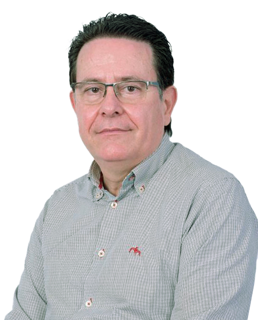
Dr. Salvador Hidalgo
Researcher
IMB-CNM address
Instituto de Microelectrónica de Barcelona (IMB) Centro Nacional de Microelectrónica (CNM)
C/ dels Til.lers s/n. Campus UAB - Bellaterra 08193 Cerdanyola del Vallès (Barcelona) Spain
Phones:
E-mail:
PROFILE
Dr Salvador Hidalgo was born in Granada (Spain) on 1961. He received the B.S. and the Ph.D. in Sciences (Physics) from Autonomous University of Barcelona in 1986 and 1990, respectively. In 1987, he joined the Institute of Microelectronics of Barcelona (IMB-CNM), belonging to the National Microelectronics Centre (CNM-CSIC), as a member of Power Semiconductor Device Group, specializing in the development of power devices with MOS gate control in vertical, lateral and trenches configuration. Between 1991 and 1993, he taught at the Faculty of Electrical Engineering of the Ramon Llull University in Barcelona, where he taught Physics, Electronics and Microelectronics for undergraduate and graduate students. In 1992, he got a permanent research position at the Spanish National Research Council (CSIC), and since 1999, he is also head of the IMB-CNM Reverse Engineering Group.
He is author of 70 publications in international SCI journals, 140 communications to international conferences (of which 7 received the award for the best paper), 65 communications to national congresses and 9 units in collective volumes of international scope. He has participated in 22 EU founded research projects, 42 funded by Spanish science and technology institutions, 50 R & D industrial contracts and 10 patent applications. He has supervised two Ph. D. Thesis and five Engineering or Master Projects. He is currently working on advanced IGBTs with monolithically integrated voltage and current sensors, Trench JFET power devices, and on silicon radiation detectors for high-energy physics. He is currently member of the New Technologies Committee of the Spanish Institute for Strategic Studies, CERN CMS experiment and RD50 and RD51 collaborations. His main scientific interest is focused in fields of the semiconductor devices and technologies, power and high voltage integrated microelectronics, power semiconductor devices and technologies, modelling of semiconductor devices and processes, low voltage protection devices, SOI/SOS fabrication techniques, radiation detectors technologies and reverse engineering processes to microelectronic devices analysis.
Google Scholar Profile

