RESEARCH AND EDUCATION
RESEARCH LINES
EDUCATION
SILICON POWER DEVICES
Design of new power structures for high efficiency converters and smart grids, with voltage capability from 600 to 6500 V. Reliability of power devices in radiation environments and design of advanced radiation detectors for tracking applications in high energy physics.
Application fields of Silicon Power Devices
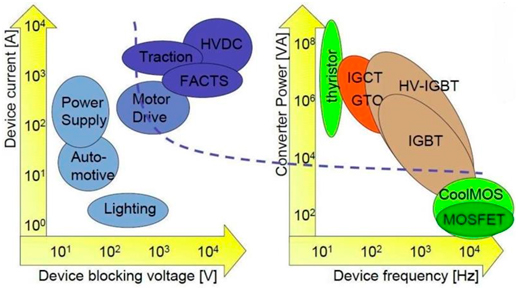
Device Design
Design and optimization of new lateral and vertical power semiconductor devices on Bulk Silicon and Silicon-on-Insulator substrates.Electrical and technological TCAD simulation.
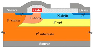
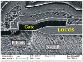
Design of an LDMOS device and its corresponding cross-section micrograph.
Super Junction Power MOSFET (600 V)
Avalanche ruggedness optimization of a new generation of 600 V SJ power MOSFETs (UltiMOS®)based on deep trench technology (ON-Semiconductor, Belgium). Technical solutions for high-energy capability under UIS stress.
UltiMOS® cross-section and uniform current distribution under a UIS test.
V=800 V and I=8 A.
Process Technologies
Set-up of process technologies in the IMB-CNM Clean Room for the fabrication of low voltage MOSFETs, high voltage IGBTs and MOS-Thyristors.Standard double diffusion VDMOS/IGBT technology.
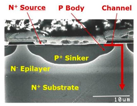
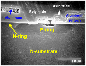
Cross-section micrographs of a VDMOS cell and a periphery termination.
3300 V – 50 A IGBT with Anode Voltage Sensor
Large area IGBT (> 1 cm²) with anode voltage sensor monolithically integrated in the active area and auxiliary cathode pad for current sensing. Short-circuit protection in traction power modules.

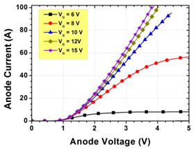
3300 V – 50 A IGBT with anode voltage and current sensors and current capability for different gate bias.
Protection devices
Very low transient voltage suppressors for integrated circuit protection, 200-1000 V diodes and rectifiers for domestic applications and auxiliary AC switches and thyristor gate firing devices (FagorElectrónicaS.Coop, Spain).
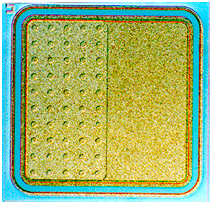
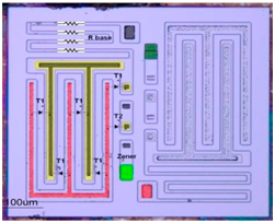
220 V bidirectional breakover diode and bilateral switch developed for FagorElectrónica.
Radiation Effects on Power Devices and Radiation Detectors
Reliability and damage analysis of power devices used in harsh environments. Design and fabrication of advanced tracking radiation detectors for high energy physics and medical applications.

Cross-section view of a Low Gain Avalanche Detector.
Low Gain Avalanche Detectors (LGAD)
Controlled avalanche process to improve performance and stability of PiN diode detectors against radiation damage, achieving a high signal to noise ratio.1100 V LGAD devices with very low leakage current and a detection area of 25 mm² with a gain in the range of 10-20.
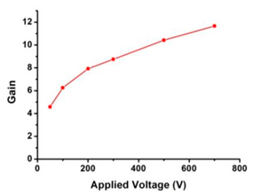
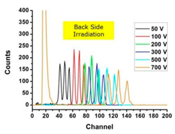
Experimental gain measurement and detected spectrum for a tri-alpha source.

