RESEARCH AND EDUCATION
RESEARCH LINES
EDUCATION
WBG SEMICONDUCTORS
Wide BandGap semiconductors research activities are focused on the development of technological processes optimized for wide gap semiconductors (SiC, GaN and diamond) and on the design and fabrication of new power devices based on these materials for high-voltage and high temperature.
Applications field of Wide Band Gap Power Devices

Comparison of Si, SiC and GaN physical parameters.
SiC full optimized technology modules allow studying a wide range of devices and sensors
Power Switches: BJT, MOS, JFET.

Micrographs of different power devices. From left to right: BJT transistor, Vertical MOSFET and JFET.

3” SiC wafer with power and test devices. SiC MOSFET with integrated sensors.
Power Rectifiers: Schottky, JBS and PiN


From left to right: High temperature packaged SiC Schottky diodes. Breakdown voltages up to 10 kV of bipolar HV SiC diodes.9 A – 2500 V switching waveforms of a 3.3 kV diode.

Typical cross-section of a JBS diode.
High Temperature sensors: Hall sensors, Gas sensors, UV detectors


From left to right: Micrograph of a SiC-based Hall magnetic sensor. Dynamic response of a SiC-based CO and NO2 gas sensor.Layout and cross-section of a SiC UV detector.
Biomedical Sensors: Impedance Needles and MEAs


Left to right: Packaged impedance needle. Impedance needles on a SiC fabricated wafer.
High Temperature Digital ICs


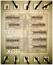
SiC-based integrated circuit implementing different logical functions.
Micro-Nano resonators


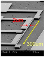
SiC-base microstructures (such as cantilevers) for MEMs applications.
High-Temperature SiC Diodes
Design and fabrication of high temperature SiC blocking diodes for solar panel arrays: series protection devices for solar cells arrays. Used in ESA space mission Bepi-Colombo (set off on a journey to Mercury lasting approximately 6 years) and Solar-Orbiter.Working temperature range -170C to +300C.High reliability, radiation hard, very stable under thermal cycling.


From left to right: 3 “ wafer with the fabricated diodes. Diode soldered on the metallic package. Top-side wire-bonding connections. View of the ESA’s Bepi-Colombo probe.
SiC-based diodes for voltage multiplier circuit
Optimized for Philips X-Ray medical equipments in the framework of ENIAC SmartPM project.


4” SiC diodes wafer.
Power circuits based on Si (left) and SiC (right) diodes.
Ramp-up at 92 kV / 42 kW.
GaN on Si HEMT Devices
Heterojunction devices AlGaN/GaN, InAlN/GaN.MIS gate.Up to 1000 V and 300ºC operation.Developed for ON-Semiconductors (Belgium).


From left to right: cross-section of the designed MIS-HEMT structure. Wafer view showing several fabricated devices including large area (20 A) transistors. Curves showing the main forward and blocking characteristics.
Graphene growth on SiC
Growth: Epitaxial growth on SiC (since 2007) and CVD growth on Cu (from 2012).


From left to right: Crystalline structure of 4H-SiC used for graphene growth. Graphene ribbon and reference grid on SiC wafer. Graphene layer growth on Cu substrate.
Processing: “Standard” processing EBL + RIE + E-gun. Best cases: n=1011 cm-2, µ=11.000 cm2/V.s at 4.2 K.


From left to right: SEM micrograph of Ti/Au contacts on graphene device. AFM image of a graphene device.

