

From August 2 to 7, 2026, the 6th International Workshop on Gallium Oxide and Related Materials (IWGO-6) was held in College Park, Maryland, USA. IWGO is one of the leading international forums devoted to Ga₂O₃ and related materials. It covers a broad range of topics, including material growth and processing, characterization, polymorphism, theoretical modelling, and electronic devices.
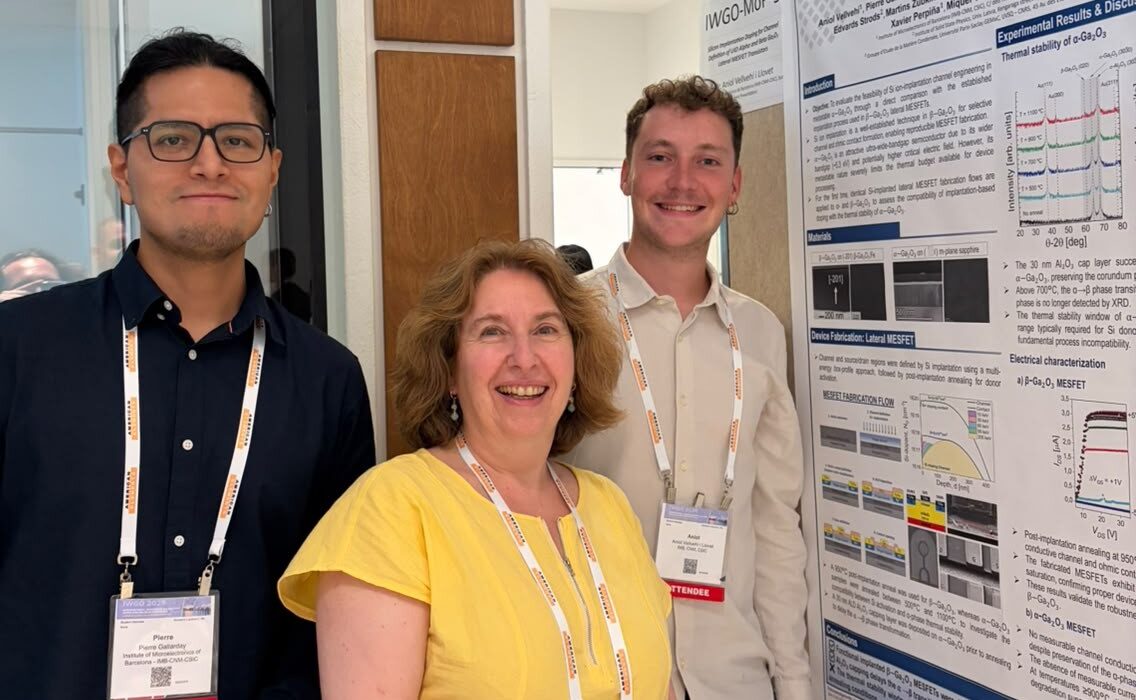
Two PDS PhD students, Pierre Gallarday and Aniol Vellvehí, presented complementary research on Ga₂O₃-based technologies. The picture above shows Pierre Gallarday and Aniol Vellvehí during their poster presentations at IWGO-6, accompanied by Ekaterine Chikoidze from GEMaC (CNRS-UVSQ, Université Paris-Saclay), one of the co-authors of the presented works.
On Monday, August 3, Aniol Vellvehí presented the poster entitled “Silicon Implantation Doping for Channel Definition of UID Alpha and Beta Ga₂O₃ Lateral MESFET Transistors.” The work compares silicon implantation for channel definition in lateral α- and β-Ga₂O₃ MESFETs fabricated using the same process. In β-Ga₂O₃, the implanted donors were successfully activated, resulting in functional and reproducible transistors. In α-Ga₂O₃, however, the temperature required for donor activation caused an α-to-β phase transformation and structural degradation. The study therefore confirms the robustness of implanted-channel engineering in β-Ga₂O₃ while revealing a fundamental thermal limitation in α-Ga₂O₃.
On Tuesday, August 4, Pierre Gallarday presented the poster entitled “Gigantic Space-Charge-Limited Currents and Thermal Effects in Si–Fe-Doped Ga₂O₃ Devices.” This work investigates unusually large space-charge-limited currents in Fe-doped β-Ga₂O₃ substrates containing a silicon-implanted conductive channel. The implantation reduces the thermal conductivity of the material, while the non-uniform electric-field distribution produces highly localized Joule heating. The resulting temperature gradients can lead to premature thermal breakdown at relatively low voltages. These findings provide new insights into electrothermal effects in Ga₂O₃ and suggest potential applications in localized solid-state heating and functional surfaces.
On Wednesday, August 5, Pierre Gallarday also gave an oral presentation entitled “Demonstration of Homojunction Ga₂O₃ PiN Diodes with High Bipolar Injection.” The work presents a new generation of vertical Ga₂O₃ homojunction PiN diodes in which phosphorus implantation is used to form a conductive p-type region. The devices demonstrate clear bipolar operation and strong conductivity modulation, achieving current densities above 6,000 A/cm², breakdown voltages exceeding 500 V, and ON/OFF ratios of up to 10⁷. These results confirm the potential of Ga₂O₃ p–n junctions for future power electronic devices.
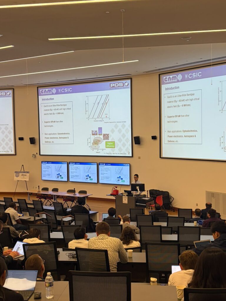
Pierre Gallarday during his oral presentation at IWGO-6.
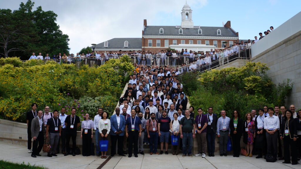
Group photo of the participants at the 6th International Workshop on Gallium Oxide and Related Materials (IWGO-6) in College Park, Maryland, USA.